
SiC Wafer Polishing
Silicon carbide (SiC) wafer polishing is a key step in the manufacture of high-performance semiconductors, especially for power electronics and high-frequency devices. SiC wafers are prized for their superior performance under extreme conditions, including high temperature and voltage. As such, SiC is ideal material for high-power electronics, renewable energy systems, electric vehicles (EVs), and aviation. The polishing process is a crucial part of producing SiC semiconductors as it guarantees their quality, performance and reliability.
The production of SiC wafers is generally done via chemical vapor deposition (CVD), or physical vapor transport (PVT), which are some of the methods for growing crystals. The result is then sliced into thin wafers from the bulk crystal where surfaces are rough and uneven, thus needing several processing stages such as lapping, grinding and polishing. Last but not least, polishing will ensure that the surface of the wafer is at an atomic level lustrous with all defects or imperfections taken care of that may hinder how well it operates in its final semiconductor device.
Polishing SiC wafers poses a great challenge because this material is extremely hard. A diamond being one of its major elements ranks among the hardest materials on Earth; hence attaining ultra-smooth surfaces required by high power electronics circuits becomes quite difficult. Traditional techniques for polishing silicon cannot be applied on SiC too, necessitating specialized techniques and equipment.
Silicon carbide (SiC) is typically manufactured via different methods that involve growing crystals such as physical vapor transport (PVT) or chemical vapor deposition (CVD) into single crystals first. Slicing from this bulk crystal leads to thin wafers whose surfaces are rough and non-uniform hence multiple stages of processing including lapping, grinding and polishing must be done. Finally, polishing removes defects or imperfections affecting electronics thereby enabling atomic-level smoothness of the wafer’s surface.
Polishing SiC wafers is especially challenging because of its hardness. For instance, silicon carbide ranks one of hardest materials known; thus it becomes more difficult to attain other required optical properties for high-performance electronics. The traditional silicon polishing techniques cannot apply to SiC therefore, specialized methods and tools have been developed to solve the problem.
The most common ways of producing silicon carbide (SiC) wafers are chemical vapour deposition (CVD) and physical vapour transfer (PVT) techniques. After slicing the bulk crystal into thin wafers, the surfaces are uneven and rough, necessitating several processing steps including lapping, grinding, and polishing. The last stage is polishing; here, the wafer's surface flaws and impurities are removed to an atomic level which has a possibility of enhancing the performance of the final semiconductor devices.
Polishing SiC wafers is very difficult because of its hardness. For high-performance devices it is difficult to achieve ultra-smooth surface as silicon carbide is one of the hardest materials known. Hence, conventional silicon wafer polishing processes are not adequate for SiC wafers and new specialized methods and tools should be developed.
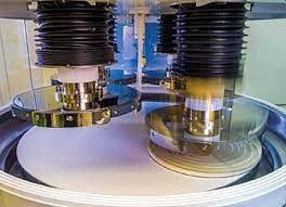
The most commonly used method for polishing SiC wafers is chemical mechanical polishing (CMP). By combining mechanical and chemical forces, CMP produces a mirror-like surface on the wafer. The method utilizes an abrasive slurry consisting of chemicals that is rubbed against the wafer on a rotating polishing pad. Atoms making up surface irregularities are wiped away while quantum roughness is erased by both the action of the pad and the reaction taking place between the slurry and the surface of the wafer.
The success of this process highly depends on how one chooses the pads and slurries to use during polishing. It is essential to design such slurries that remove materials effectively without resulting into extra damages or introducing new defects. This means that pads must be selected taking into account their durability, hardness, and appropriateness.
SiC wafer polishing is an arduous task due to numerous reasons, the most important being natural hardness of the material and the need for extremely fine surface quality control. Such surface roughness levels are usually in a few nanometres range which necessitates sophisticated machinery and strictly regulated processes. Additionally, any defects like pits, scratches or subsurface damage can adversely affect performance of the finished device hence defect management becomes vital during polishing process.
Another challenge is its cost. The difficulties in growing large superior SiC crystals and complex polishing processes make SiC wafers more expensive than standard silicon ones. With increasing demand for SiC devices particularly in industries such as power electronics and electric vehicles, it’s possible to achieve reduced production costs through improved wafer technology.