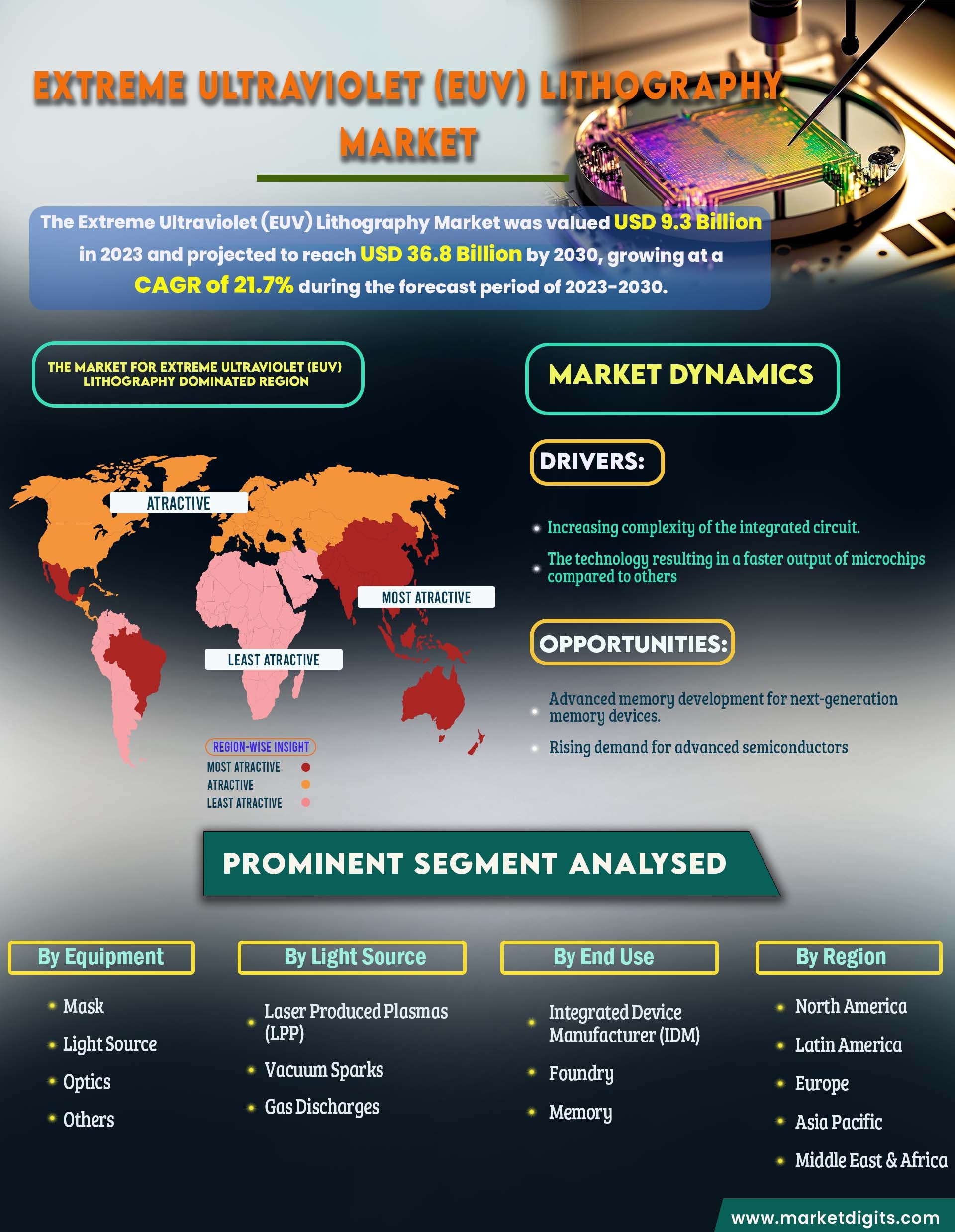
 Extreme ultraviolet lithography (EUVL) is a cutting-edge technology used in the semiconductor industry to manufacture integrated circuits. It employs extreme ultraviolet (EUV) light with a wavelength of 13.5 nanometers to create intricate patterns on silicon wafers. This process is crucial for producing the latest generations of microchips, enabling the continuation of Moore’s Law, which predicts the doubling of transistors on a chip approximately every two years. EUVL uses a high-powered laser to generate plasma from tin droplets, which then emit EUV light. This light is collected and focused using ultra-flat mirrors in a vacuum chamber to project the desired circuit patterns onto a photoresist-coated wafer. The technology allows for the creation of smaller, more efficient, and more powerful chips, essential for advancements in computing and electronics. Despite its complexity and high cost, EUVL is indispensable for the production of chips with features as small as 5 nanometers and below. Companies like ASML are at the forefront of developing and supplying EUV lithography systems, making significant contributions to the semiconductor industry’s progress. As the demand for more powerful and compact electronic devices grows, EUVL remains a pivotal technology in meeting these needs.

البحث
الأقسام
- Politics
- الرئيسية
- Wellness
- Theater
- Sports
- Shopping
- Religion
- Party
- أخرى
- Networking
- Music
- Literature
- Art
- Health
- Gardening
- الألعاب
- Food
- Fitness
- Film
- Drinks
- Dance
- Crafts
- Causes
إقرأ المزيد
Tiffany 鑽石項鍊:優雅與永恆的完美象徵
在眾多珠寶品牌中,Tiffany 始終是優雅與奢華的代名詞。創立於1837年的 Tiffany &...
LiDAR Filters Market | Industry Analysis, Emerging Demands and Forecast to 2031 |
LiDAR Filters Market report has recently added by Analytic Insights Hub which helps to make...
Polysilicon Market 2024: Analysis, Growth, Size, Trends And Forecast 2030
Polysilicon Industry
The global polysilicon market is anticipated to reach USD 104.69 billion by...
KONSTANT Mini Dumper Ideal for Narrow Terrain Transport Jobs
Whether on construction sites, agricultural fields, or landscaping projects, the Mini...
Why YES Germany is Considered a Top Educational Consultancy in Coimbatore
When it comes to pursuing higher education abroad, especially in Germany, students in Coimbatore...